CPU Design on FPGA
Graduation project · Uludağ University — a processor built from logic gates to Verilog
How does a processor actually work? For my graduation project I answered that from first principles: starting at semiconductors, logic gates and Boolean algebra, and ending with a complete CPU described in Verilog and synthesized for an Intel FPGA.
Following the SAP (Simple-As-Possible) approach of Malvino's Digital Computer Electronics, the ALU and the microcoded control unit were first designed gate-by-gate in Multisim as 4-bit prototypes. The full architecture — registers, program counter, memory and datapath — was then written as Verilog modules and taken through synthesis, RTL inspection and waveform simulation in Quartus Prime.
Architecture
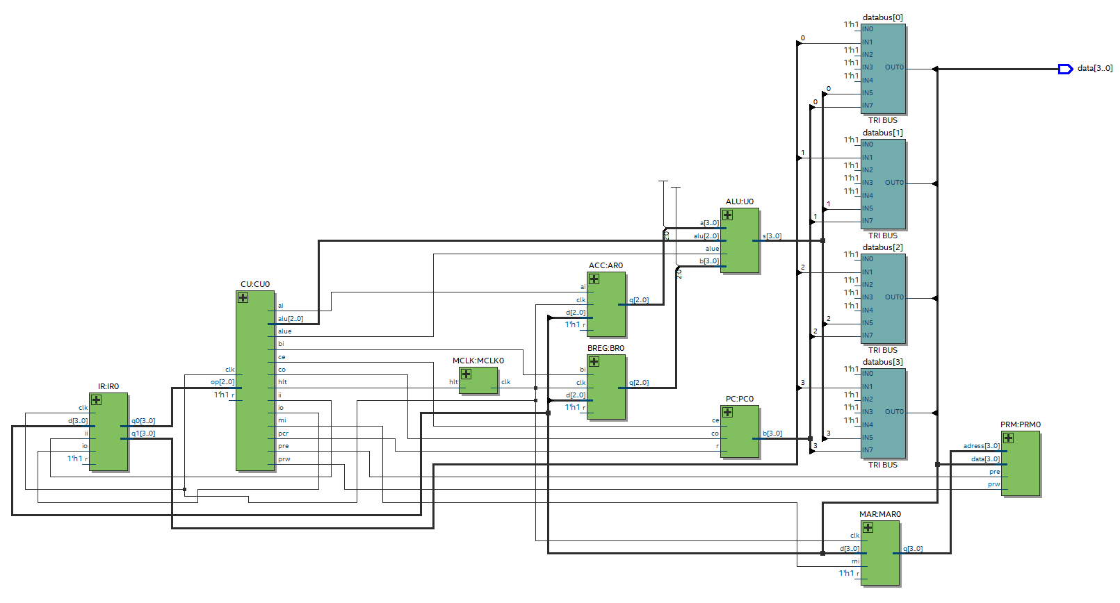
- Bus-based design: accumulator, B register, instruction register, MAR, program counter and program memory share a tri-state data bus.
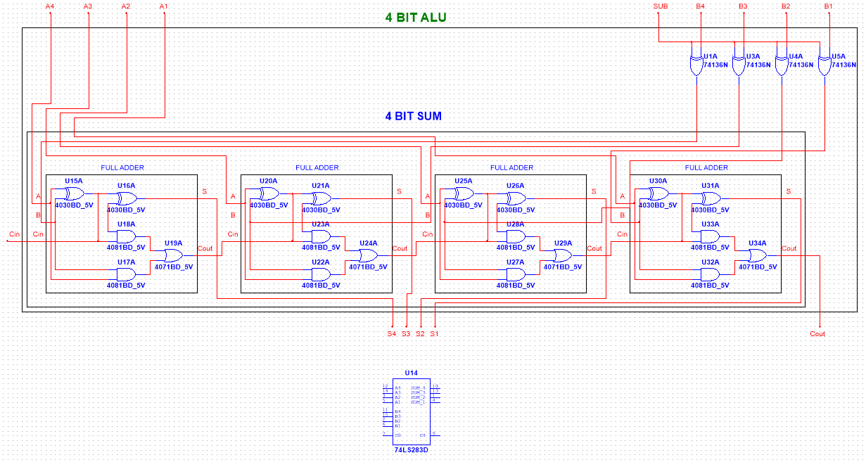
- The ALU adds and subtracts with four full adders; XOR gates invert the B operand for two's-complement subtraction.
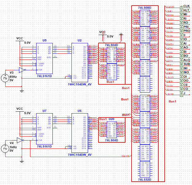
- The control unit steps through fetch–decode–execute with 74LS161 counters and 74HC154 decoders, generating the CPU's control signals.
- Every instruction is microcode — LDA: CO MI · PRO II · CE · IO MI · RO AI — building up a ~9-opcode instruction library.
Design flow
Gate-level ALU
4-bit ALU built from full adders in Multisim, with XOR-controlled subtraction
Multisim / TTLControl unit & microcode
A counter + decoder matrix generates the control signals; LDA's microcode worked through step by step
74LS161 · 74HC154Verilog implementation
The CPU split into modules — ALU, ACC, B register, IR, MAR, PC, program memory and control unit
VerilogSynthesis & RTL review
Design synthesized for a Cyclone 10 LP; the datapath inspected in the RTL viewer
Quartus PrimeSimulation & verification
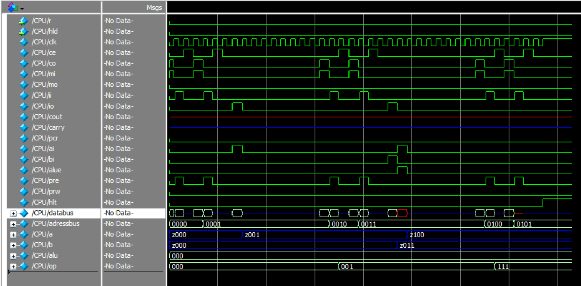
Fetch–execute cycles verified on waveforms; unknown bus states flagged for design fixes
ModelSim / Altera SimFrom the thesis